What is Hammer?
Taping out chips is a pain - let's fix that. Hammer tames the complexity of the EDA design process, EDA tools, and PDKs, in order to allow designers to easily accomplish common physical design tasks.
Hammer has been used in over seven (7) chip projects in different technology nodes (from 28nm to 16nm), design architectures (embedded mixed-signal processors to multi-core RISC-V processors with high-speed serial links), and different EDA tools.

Getting Started
To get started with Hammer, you can find documentation and tutorials at docs.hammer-eda.org. The Hammer codebase is open-source and lives at https://github.com/ucb-bar/hammer.
Join us at the Hammer mailing list if you have any questions or need help.
EDA CAD Plugins
UC Berkeley maintains a selection of EDA CAD vendor plugins, and can distribute them with approval from the relevant vendors. If you are a university or company with licensed access to EDA CAD tools, please contact us at hammer-plugins-access@lists.berkeley.edu to request access to the plugins.
We are also working on an OpenROAD plugin.
Technology PDK Plugins
Hammer supports NanGate45 and the ASAP7 PDK out of the box.
Unfortunately, UC Berkeley is not able to distribute any proprietary technology plugins under its current licensing/legal arrangement.
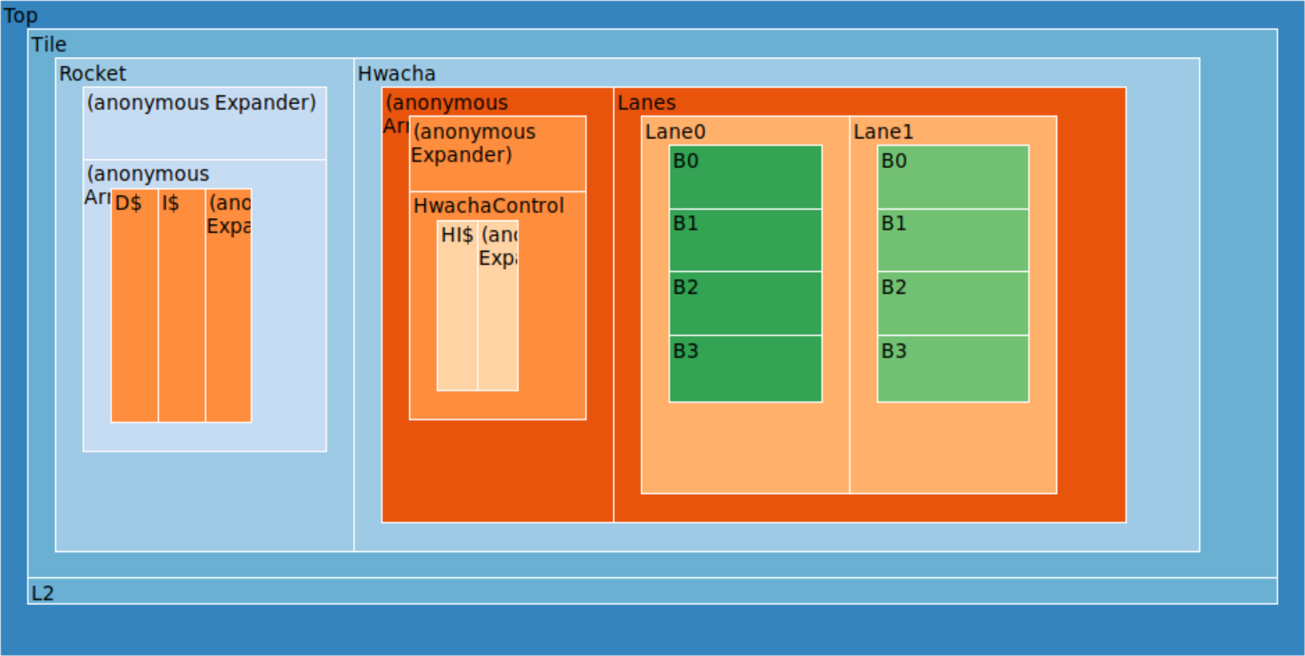
Chipyard
Hammer is also an integral component of the Chipyard framework from UC Berkeley Architecture Research. Useful documentation for how an example block is pushed through the VLSI flow with Hammer in the free ASAP7 PDK in Chipyard is at https://chipyard.readthedocs.io/en/latest/VLSI.
Acknowledgements
If you use Hammer in your work, please cite the following paper:
Edward Wang, Colin Schmidt, Adam Izraelevitz, John Wright, Borivoje Nikolić, Elad Alon, Jonathan Bachrach. “A Methodology for Reusable Physical Design”. In proceedings of the 21st International Symposium on Quality Electronic Design (ISQED 2020), Santa Clara, USA, March 2020.